
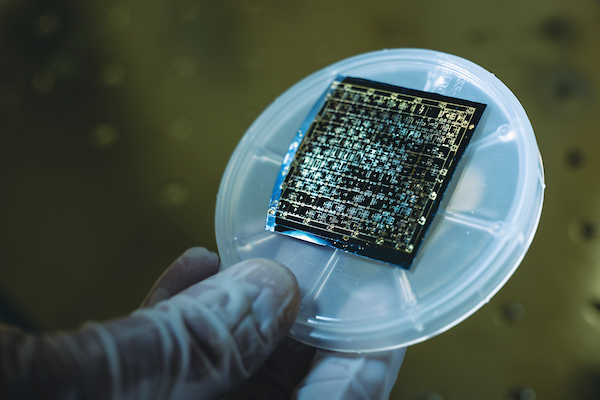
Microelectronics
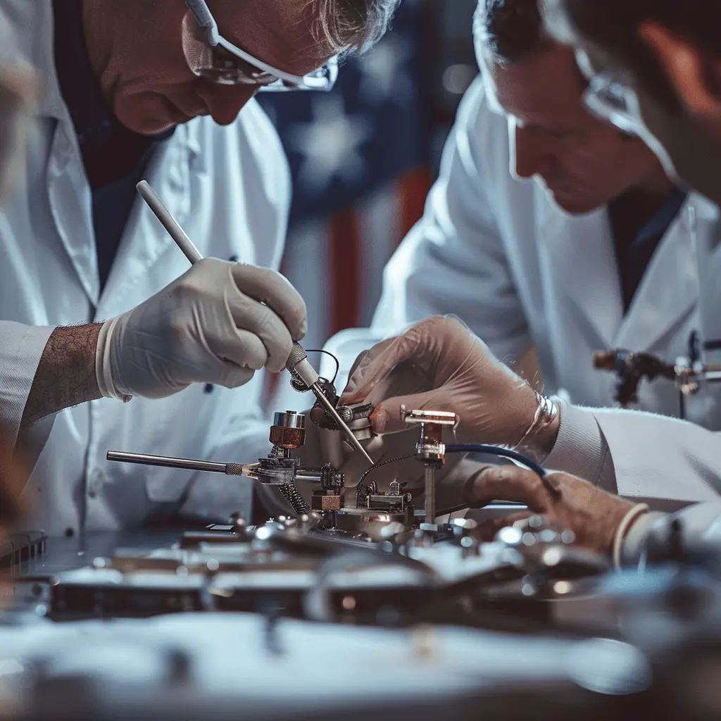
The PARI Microelectronics Lab (PML) reinforces this critical science as the linchpin of national security, cutting across important areas from weapons systems to infrastructure.


THE PML DIFFERENCE
Microelectronics are the backbone of modern defense, powering weapons systems, information and sensing technologies, critical infrastructure and space-based capabilities.
PARI Microelectronics Lab (PML) advances technologies that safeguard the nation. Through cross-functional teams and end-to-end research, PML designs, builds and delivers state-of-the-art microelectronic solutions that tackle the most complex national security challenges.
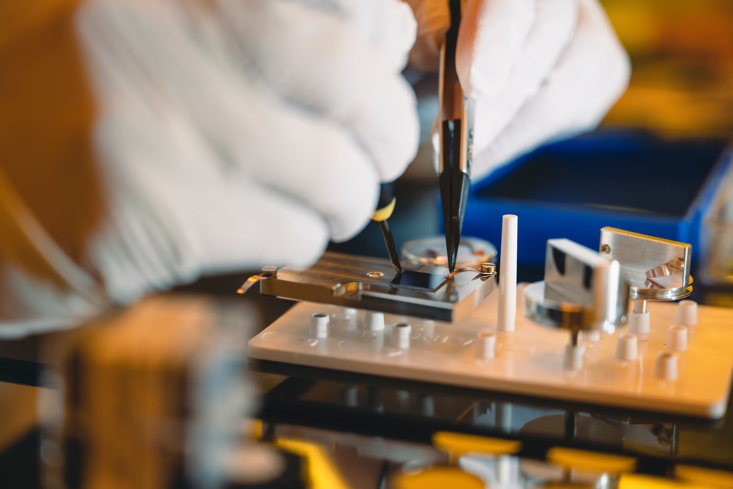
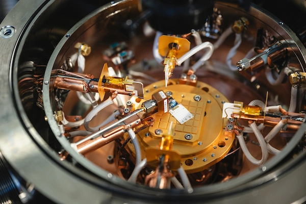
Microelectronics in extreme environments
Radiation hardened, radiation tolerant and other high-temperature chips for applications such hypersonics and space.
Materials and processes
Optimizing microelectronics fabrications and facilities to best meet national security needs.
Modeling and Simulation
Create data sets that influence decision making for state-of-the-art applications.
SIlicon Photonics
Develop sensing, biomedical, automotive, astronomy, aerospace, augmented reality, virtual reality, and artificial intelligence applications
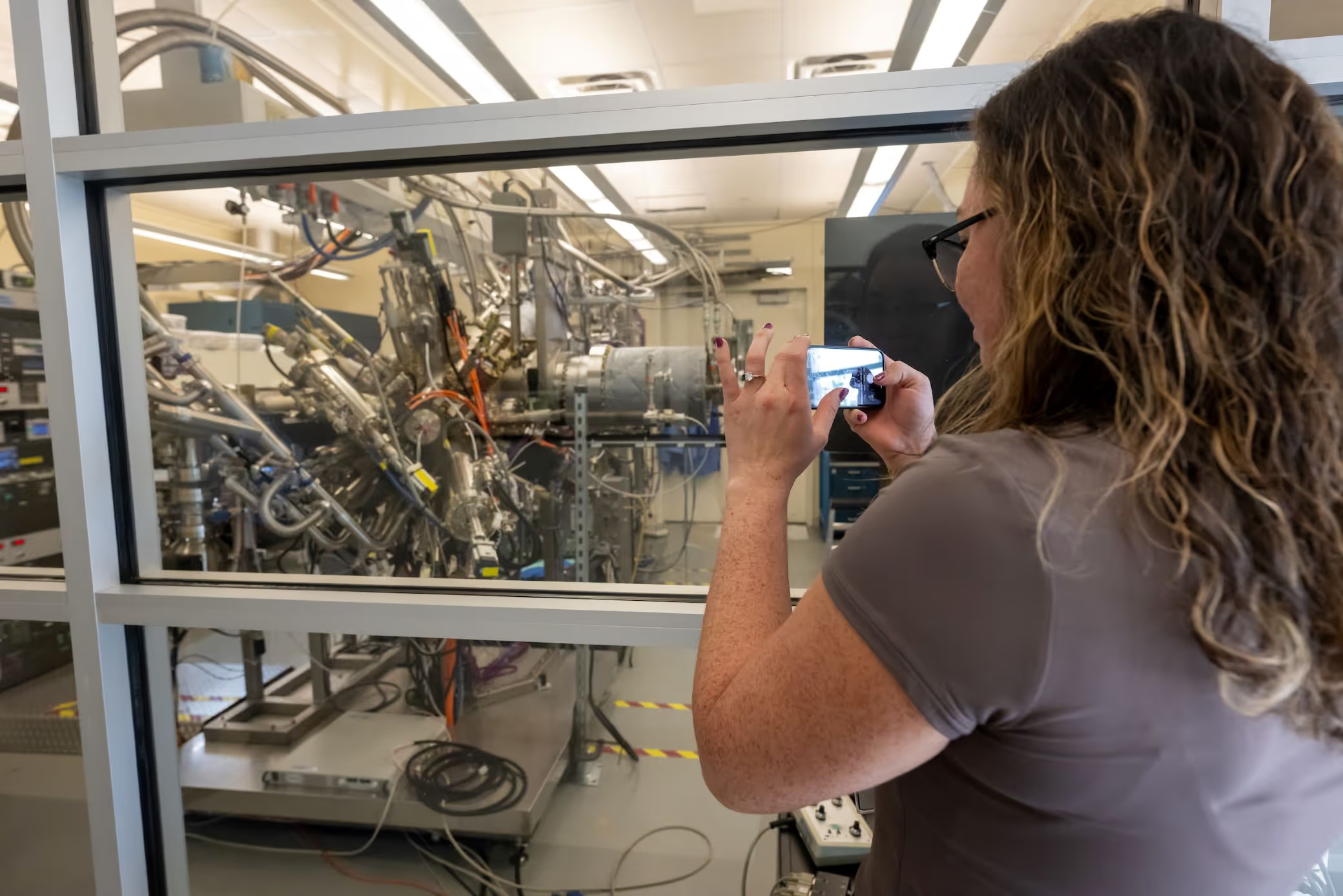
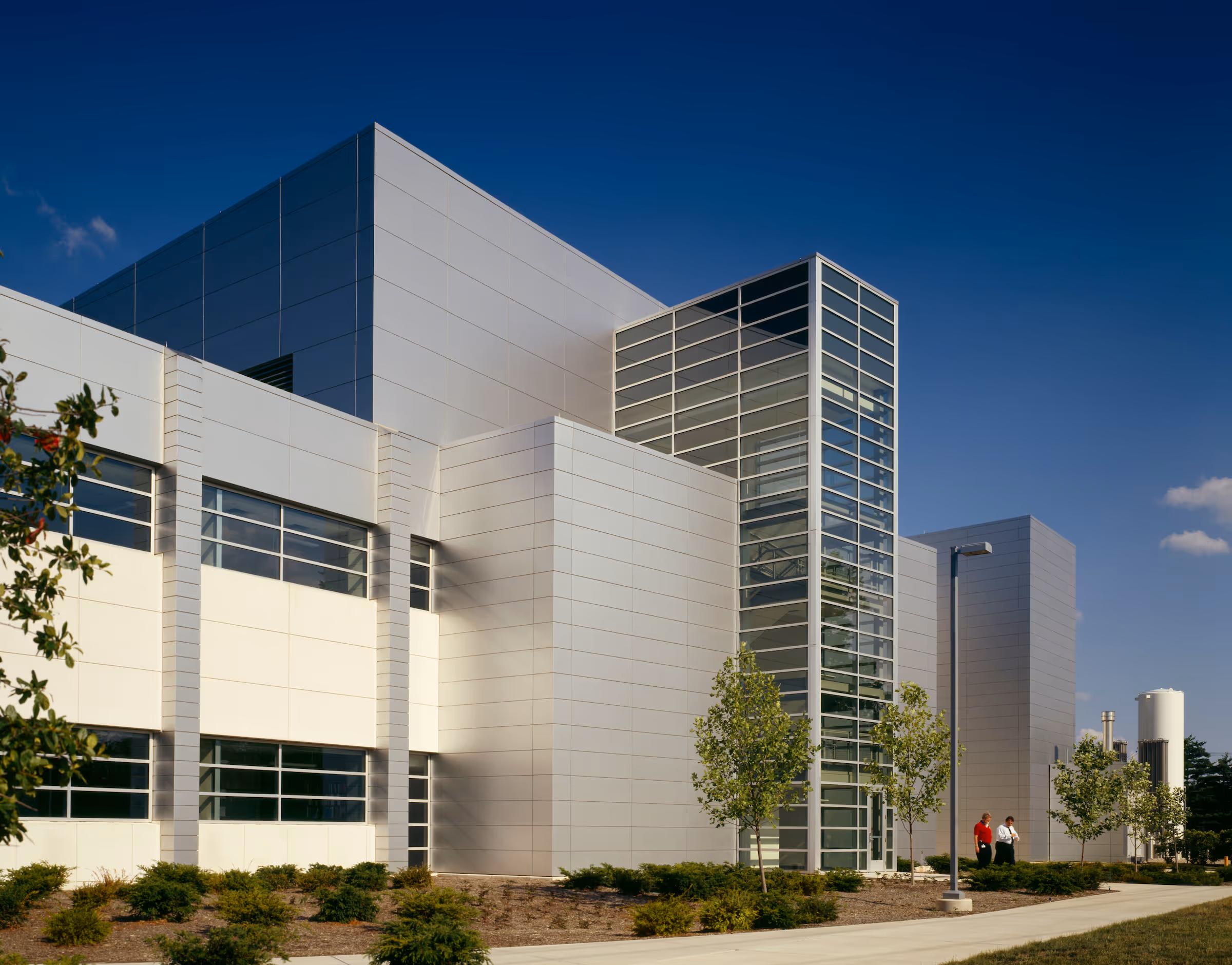
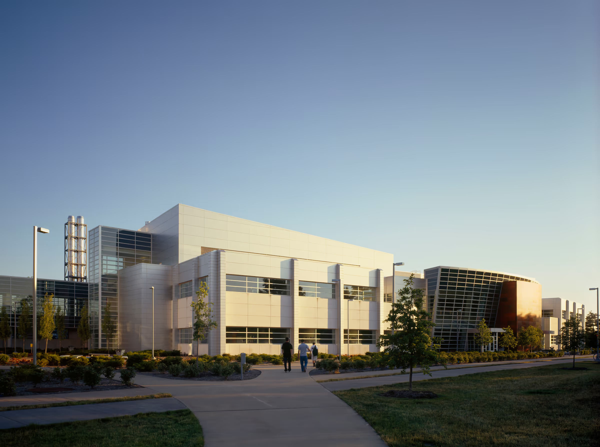
Facilities/Capabilities
PML works in new laboratories and facilities in renovated and accredited spaces for classified U.S. government work.
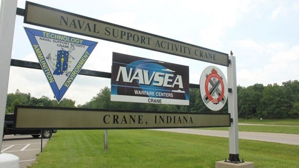
Naval Surface Warfare Center, Crane Division, Odon, IN
- Third largest naval warfare center in the world. Crane oversees multidomain, multispectral, full life cycle support of technologies and systems enhancing capability to today’s Warfighter.
- Member of the Indiana Research Consortium, a research engine of Indiana’s three largest research universities to drive innovations and advancements in critical national security areas. As part of this effort, this hub for defense research will address challenges in microelectronics and workforce development.
- More info here.
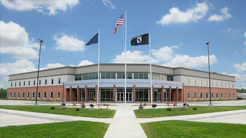
WestGate@Crane Technology Park, Odon, IN
- Home to the $2 billion Microelectronic Commons Program, established through NSWC Crane and managed by the National Security Technology Accelerator. It enables lab-to-fab transition of microelectronics innovations; enables cost-effective exploration of new materials, devices, architectures, and prototyping in domestic facilities; accelerates transition of new technologies to domestic manufacturers.
- Home to NHanced Semiconductors, a design and manufacturing innovator of semiconductor technologies. Mid-volume production, low-volume advanced package assembly and workforce training are at this location.
- Robust supply-chain and other expertise across multiple areas.
- More info here.
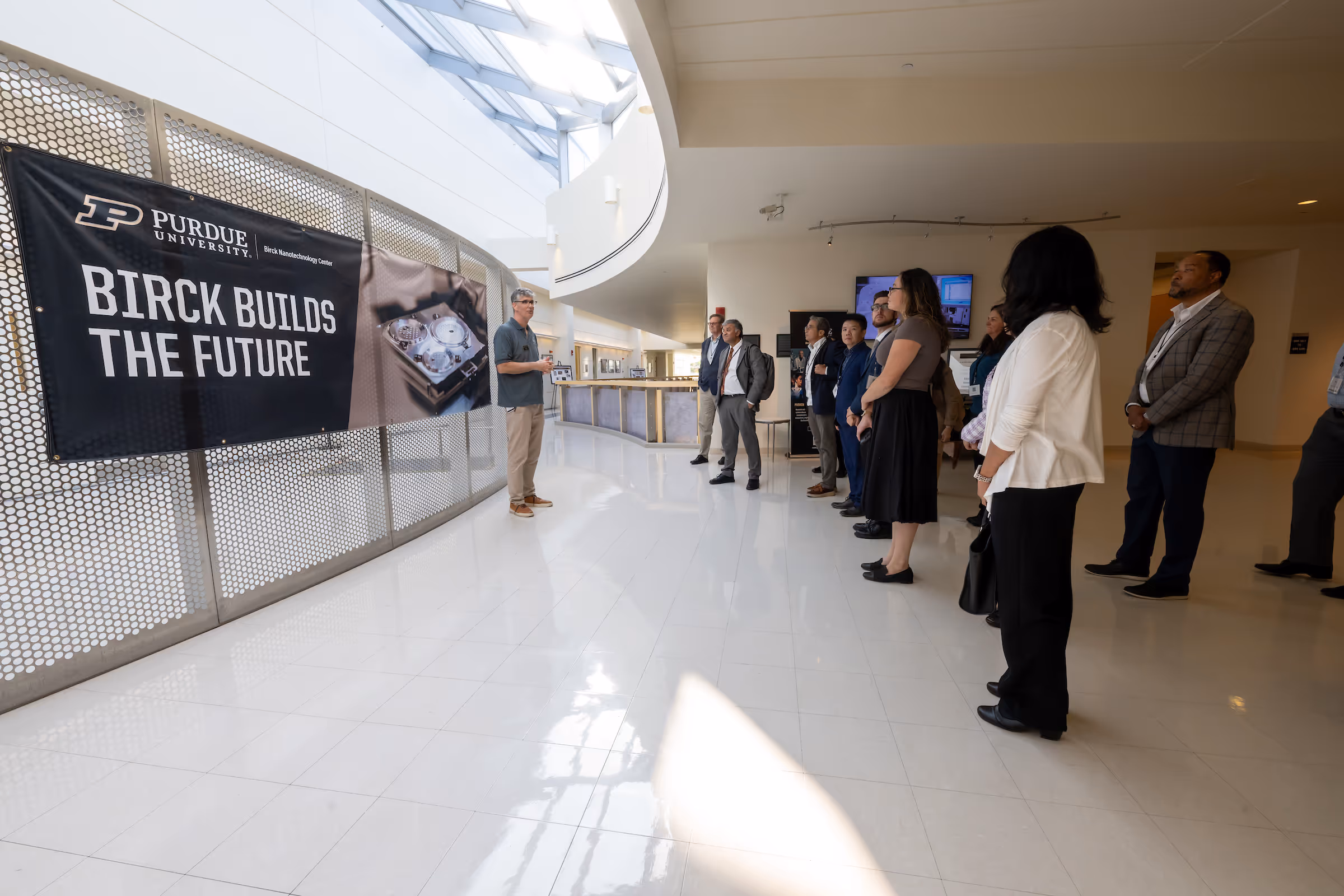
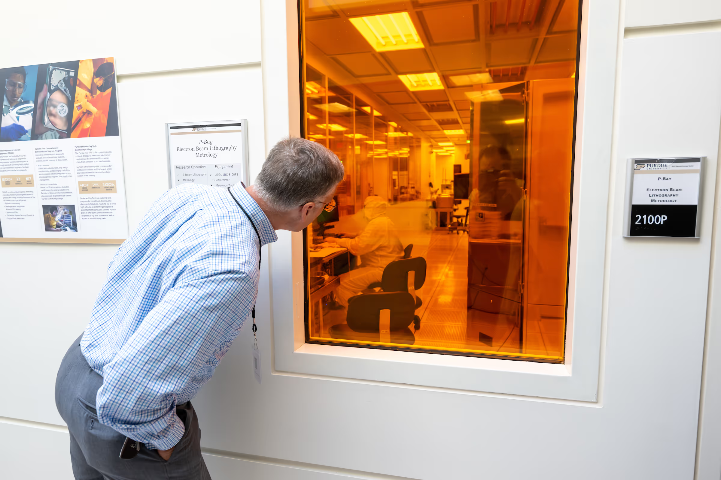
Birck Nanotechnology Center, Purdue University, West Lafayette, IN
- Scifres Nanofabrication Laboratory, a 25,000-square-foot cleanroom, the second largest in this country
- 33,000 square feet of specialized laboratories for device and materials characterization
- Home to Purdue’s advanced research and development on semiconductors and other technology at the atomic scale
- Equipment for lithography, etching, epitaxy, processing and packaging.
- Classified laboratory space and meeting rooms.
- More info here.
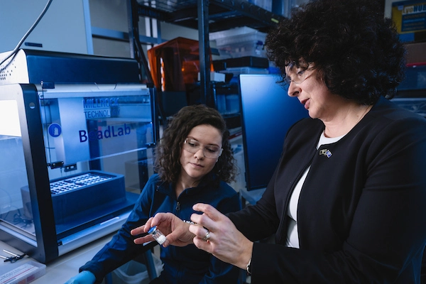
Our People


Ready to Move at Mission Speed?
Whether you're facing a classified challenge or an unclassified opportunity, PARI has the people, facilities, and commitment to deliver.